opensource.google.com

Menu
Showing posts with label hardware. Show all posts

Open source PDKs joining the Linux Foundation’s CHIPS Alliance

Wednesday, November 8, 2023

In November 2020, we launched our Open Source MPW Shuttle Program to make it easier for researchers and developers to build custom silicon and to enable a thriving ecosystem around open source hardware. Working with our partner, SkyWater Technology, we released the first foundry-supported open source process design kit (PDK) for their 130nm mixed-signal CMOS technology (SKY130), then welcomed GlobalFoundries as a partner with the release of an open source PDK for their 180nm MCU process (GF180MCU).

Then, to give researchers and developers a way to validate and prove their designs made with the PDKs, we partnered with Efabless to fund a series of no-cost manufacturing shuttles for open source designs. In support of this program, Efabless released an end-to-end RTL to GDS design stack called OpenLane that is open source, freely available, and fully supported by their manufacturing platform. OpenLane is now being maintained as part of the OpenROAD Project. When combined with open source PDKs, a design’s verification results can now be freely shared and easily replicated by other researchers and developers, which has enabled a new collaborative model to evaluate and iterate on ideas.

Pictures of a full wafer from the first SKY130 shuttle, a tray of bare dies, and a project bring-up from SKY130 MPW-2.

Results

The Open Source MPW Shuttle Program has been a success and we’re excited by the growth we’ve seen in this ecosystem. Since its inception, the program has launched eight shuttle runs on SKY130 and an initial test run on GF180MCU, the last of which are being packaged now. With 40 slots per shuttle, we’ve manufactured 360 designs out of over 600 submissions from 19 countries around the world.Graph showing number of designs submitted to Open Source MPW shuttles across versions 1 through 8

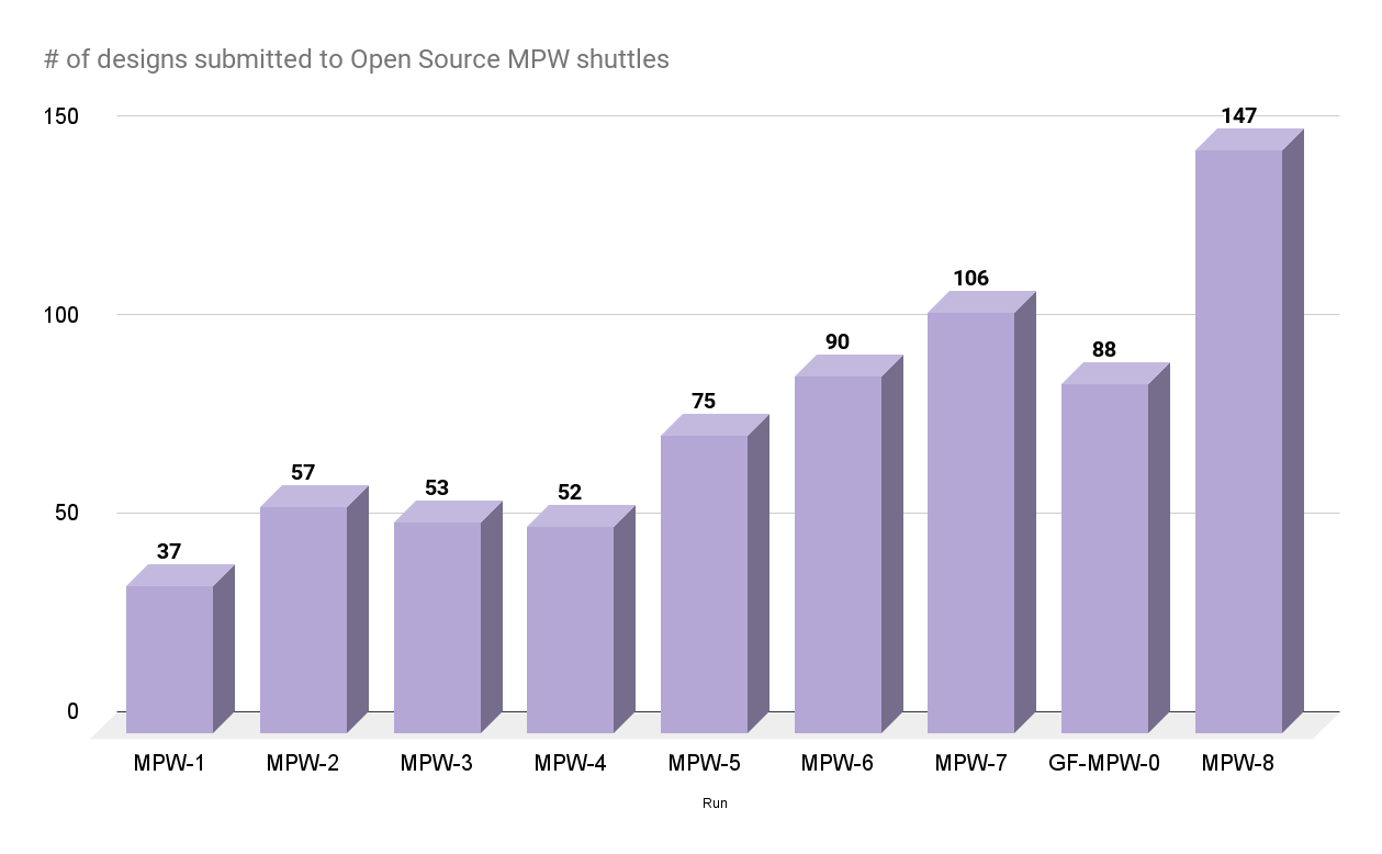
The program has also fostered collaboration between the open source community and Google. We’ve learned valuable lessons from designers who participated in the program giving feedback and filing hundreds of bugs and pull requests. These have helped to improve each successive run and to make the platforms and tools more feature-complete.

Elsewhere in the ecosystem, we’re excited by the release of new open source PDKs from foundries like the 130nm BiCMOS process from IHP, the SOI-CMOS PDK from Minimal Fab, and also by the publication of new semiconductor research using open source PDKs. Multiple universities have incorporated open source PDKs into their curriculum, and last year, NIST adopted the SKY130 PDK to migrate their existing planarized wafer designs for nanotechnology research.

Announcing GF180MCU MPW-1

We’ve just launched a new MPW-1 shuttle for GF180MCU in our partnership with Efabless. Submissions will be accepted until December 11th, targeting delivery in early 2024.

Graph showing number of designs submitted to Open Source MPW shuttles across versions 1 through 8

Next Steps

The open source silicon ecosystem is continuing to grow and evolve. After GF180 MPW-1 concludes, the open source SKY130 and GF180MCU PDKs will be joining the Linux Foundation’s CHIPS Alliance under a new working group to foster continued open source PDK development, and we expect future PDK releases will join as well. This will help with the transition to a broader governance model that enables more participation by industry, academia and the community, opening the possibility for larger shuttle programs with multiple sponsors as the ecosystem continues to grow.

Low-cost manufacturing options will continue to be available through this transition, both through commercial shuttle offerings like Efabless’ ChipIgnite program and also through educational efforts like TinyTapeout.

Thank you

Lastly, we’d like to thank the open source community. Your feedback has been invaluable to the success so far, and has helped to improve the tools and documentation to be more user-friendly. We have also seen contributions from the community in the form of hundreds of new and fully manufacturable designs, which have helped to expand the range and capabilities of open source hardware available to the community. We look forward to continuing partnerships to build a thriving ecosystem around open source silicon.

By Aaron Cunningham – Technical Program Manager, Core Hardware Tools

PJRT: Simplifying ML Hardware and Framework Integration

Monday, May 8, 2023

Infrastructure fragmentation in Machine Learning (ML) across frameworks, compilers, and runtimes makes developing new hardware and toolchains challenging. This inhibits the industry’s ability to quickly productionize ML-driven advancements. To simplify the growing complexity of ML workload execution across hardware and frameworks, we are excited to introduce PJRT and open source it as part of the recently available OpenXLA Project.

PJRT (used in conjunction with OpenXLA’s StableHLO) provides a hardware- and framework-independent interface for compilers and runtimes. It simplifies the integration of hardware with frameworks, accelerating framework coverage for the hardware, and thus hardware targetability for workload execution.

PJRT is the primary interface for TensorFlow and JAX and fully supported for PyTorch, and is well integrated with the OpenXLA ecosystem to execute workloads on TPU, GPU, and CPU. It is also the default runtime execution path for most of Google’s internal production workloads. The toolchain-independent architecture of PJRT allows it to be leveraged by any hardware, framework, or compiler, with extensibility for unique features. With this open-source release, we're excited to allow anyone to begin leveraging PJRT for their own devices.

If you’re developing an ML hardware accelerator or developing your own compiler and runtime, check out the PJRT source code on GitHub and sign up for the OpenXLA mailing list to quickly bootstrap your work.

Vision: Simplifying ML Hardware and Framework Integration

We are entering a world of ambient experiences where intelligent apps and devices surround us, from edge to the cloud, in a range of environments and scales. ML workload execution currently supports a combinatorial matrix of hardware, frameworks, and workflows, mostly through tight vertical integrations. Examples of such vertical integrations include specific kernels for TPU versus GPU, specific toolchains to train and serve in TensorFlow versus PyTorch. These bespoke 1:1 integrations are perfectly valid solutions but promote lock-in, inhibit innovation, and are expensive to maintain. This problem of a fragmented software stack is compounded over time as different computing hardware needs to be supported.

A variety of ML hardware exists today and hardware diversity is expected to increase in the future. ML users have options and they want to exercise them seamlessly: users want to train a large language model (LLM) on TPU in the Cloud, batch infer on GPU or even CPU, distill, quantize, and finally serve them on mobile processors. Our goal is to solve the challenge of making ML workloads portable across hardware by making it easy to integrate the hardware into the ML infrastructure (framework, compiler, runtime).

Portability: Seamless Execution

The workflow to enable this vision with PJRT is as follows (shown in Figure 1):

  1. The hardware-specific compiler and runtime provider implement the PJRT API, package it as a plugin containing the compiler and runtime hooks, and register it with the frameworks. The implementation can be opaque to the frameworks.
  2. The frameworks discover and load one or multiple PJRT plugins as dynamic libraries targeting the hardware on which to execute the workload.
  3. That’s it! Execute the workload from the framework onto the target hardware.

The PJRT API will be backward compatible. The plugin would not need to change often and would be able to do version-checking for features.

Diagram of PJRT architecture
Figure 1: To target specific hardware, provide an implementation of the PJRT API to package a compiler and runtime plugin that can be called by the framework.

Cohesive Ecosystem

As a foundational pillar of the OpenXLA Project, PJRT is well-integrated with projects within the OpenXLA Project including StableHLO and the OpenXLA compilers (XLA, IREE). It is the primary interface for TensorFlow and JAX and fully supported for PyTorch through PyTorch/XLA. It provides the hardware interface layer in solving the combinatorial framework x hardware ML infrastructure fragmentation (see Figure 2).

Diagram of PJRT hardware interface layer
Figure 2: PJRT provides the hardware interface layer in solving the combinatorial framework x hardware ML infrastructure fragmentation, well-integrated with OpenXLA.

Toolchain Independent

PJRT is hardware and framework independent. With framework integration through the self-contained IR StableHLO, PJRT is not coupled with a specific compiler, and can be used outside of the OpenXLA ecosystem, including with other proprietary compilers. The public availability and toolchain-independent architecture allows it to be used by any hardware, framework or compiler, with extensibility for unique features. If you are developing an ML hardware accelerator, compiler, or runtime targeting any hardware, or converging siloed toolchains to solve infrastructure fragmentation, PJRT can minimize bespoke hardware and framework integration, providing greater coverage and improving time-to-market at lower development cost.

Driving Impact with Collaboration

Industry partners such as Intel and others have already adopted PJRT.

Intel

Intel is leveraging PJRT in Intel® Extension for TensorFlow to provide the Intel GPU backend for TensorFlow and JAX. This implementation is based on the PJRT plugin mechanism (see RFC). Check out how this greatly simplifies the framework and hardware integration with this example of executing a JAX program on Intel GPU.

"At Intel, we share Google's vision of modular interfaces to make integration easier and enable faster, framework-independent development. Similar in design to the PluggableDevice mechanism, PJRT is a pluggable interface that allows us to easily compile and execute XLA's High Level Operations on Intel devices. Its simple design allowed us to quickly integrate it into our systems and start running JAX workloads on Intel® GPUs within just a few months. PJRT enables us to more efficiently deliver hardware acceleration and oneAPI-powered AI software optimizations to developers using a wide range of AI Frameworks." - Wei Li, VP and GM, Artificial Intelligence and Analytics, Intel.

Technology Leader

We’re also working with a technology leader to leverage PJRT to provide the backend targeting their proprietary processor for JAX. More details on this to follow soon.

Get Involved

PJRT is available on GitHub: source code for the API and a reference openxla-pjrt-plugin, and integration guides. If you develop ML frameworks, compilers, or runtimes, or are interested in improving portability of workloads across hardware, we want your feedback. We encourage you to contribute code, design ideas, and feature suggestions. We also invite you to join the OpenXLA mailing list to stay updated with the latest product and community announcements and to help shape the future of an interoperable ML infrastructure.

Acknowledgements

Allen Hutchison, Andrew Leaver, Chuanhao Zhuge, Jack Cao, Jacques Pienaar, Jieying Luo, Penporn Koanantakool, Peter Hawkins, Robert Hundt, Russell Power, Sagarika Chalasani, Skye Wanderman-Milne, Stella Laurenzo, Will Cromar, Xiao Yu.

By Aman Verma, Product Manager, Machine Learning Infrastructure

Google and NIST partner on nanotechnology development platform

Tuesday, September 13, 2022

We’re proud to announce Google’s cooperative research and development agreement with the U.S. National Institute of Standards and Technology (NIST) to develop an open source testbed for nanotechnology research and development for American universities. NIST—a bureau of the U.S. Department of Commerce—will start by migrating their existing planarized wafer designs to an open source framework, which can be manufactured in the U.S. on SkyWater Technologies’ open source 130nm process (SKY130). The physical wafers and source code will be available in the coming months. Together, NIST, Google, and the open source community will develop designs to facilitate research into both basic and applied science, including technology transfer into production with U.S. manufacturers.

Furthering Google’s goals to improve access to semiconductor technology, this agreement will provide academic researchers with unprecedented resources from a semiconductor foundry to enhance research into the physics of semiconductors and nanodevices. This includes their chemistry, defects, electrical properties, high frequency operation, and switching behavior, while reducing overall costs through economies of scale. Most importantly, this access enhances the technology transfer process by enabling researchers to develop new and emerging technologies using foundry resources, that can then be seamlessly transitioned into mass production since universities will already be using an industrially relevant platform. This will greatly improve scientist’s ability to move their technologies through the tech-transfer “valley of death” and into practical use.

Nanotechnology research has benefitted from silicon wafers that are normally used for chip manufacturing in a unique way. Instead of turning them into packaged microchips, their smooth, planarized surface makes a great substrate for building and testing nanoscale structures. This likewise helps test their transition into mass production.

Picture of a full wafer using the SKY130 open source PDK.

Picture of a full wafer using the SKY130 open source PDK.


The wafer for this platform has a number of different metrology structures, from parametric test structures based on simple transistor arrays—which can be probed in a probe station—to thousands of complex measurements that users can operate using synthesized digital circuits. Critically, the wafers will be available to universities in a 200 mm form factor, and mid-production planarized wafers with less than a single nanometer of surface roughness. Smooth, flat surfaces are critical for advanced manufacturing at small sizes.

NIST researchers are also ensuring that the wafers have photolithographic and electron beam alignment marks commonly found in university nanofabrication facilities, allowing the foundry silicon to be used directly by university researchers with ease. Metal pads on the surface will allow scientists to access the semiconductor transistors from the surface.

NIST scientists anticipate the nanotechnology accelerator platform will enhance scientific investigations into a diverse set of technologies, including memory devices (resistive switches, magnetic tunnel junctions, flash memories), artificial intelligence, plasmonics, semiconductor bioelectronics, thin film transistors and even quantum information science.

Picture of a development die from Google 's OpenMPW program for the nanotechnology accelerator developed by NIST and the University of Michigan

Picture of a development die from Google 's OpenMPW program for the nanotechnology accelerator developed by NIST and the University of Michigan

This program also benefits from Google’s previous contributions and support of the GDSFactory and OpenFASOC open source projects that help automate and shorten the construction of these important measuring devices from months to days. Ahead of the full wafer tapeout in 2023, NIST scientists, working with partners at the University of Michigan, Carnegie Mellon, University of Maryland, The George Washington University, and Brown University have been using Google's OpenMPW program to develop and test preliminary circuits which they expect to include in the nanotechnology accelerator. Preliminary testing will help ensure the program’s goals are met with working circuits that best serve the scientific community.

A key factor in cutting-edge research is reproducibility, or the ability for researchers from different institutions to repeat each other’s experiments and improve upon them. By migrating to an open source framework, researchers can more easily share reproducible results, contribute to the creation of open source datasets to enhance future simulation, and advance the scientific community’s state of the art of nanotechnology and semiconductor manufacturing.

NIST and Google will distribute the first production run of wafers to leading U.S. universities. Post-program, American scientists will be able to directly purchase the wafers from Skywater without license requirements, giving them the freedom to pursue their research without any restrictions. Since wafers are hundreds of times cheaper than full mask-sets or the cost of designing integrated circuits from scratch, scientists will have a much easier time getting and using this powerful industrial technology. Longer term, working with NIST to develop future platforms on the recently announced SKY90FD open source PDK will further expand this R&D ecosystem.

To kick off this research effort NIST is organizing the "NIST Integrated Circuits for Metrology Workshop" from September 20–21, 2022. This workshop will be held online with a series of presentations and panel discussions on the first day. During the second day, a working group of researchers, scientists and engineers will work to focus on the creation of parametric test structures for monolithic integration using open source silicon technology. Visit the event website to get more details about this program and register to attend or learn more about presenting.

By Ethan Mahintorabi, Software Engineer and Johan Euphrosine, Developer Programs Engineer – Hardware Toolchains Team, and Aaron Cunningham, Technical Program Manager – Google Open Source Programs Office

Open source SystemVerilog tools in ASIC design

Thursday, September 16, 2021

Open source hardware is undeniably undergoing a renaissance whose origin can be traced to the establishment of RISC-V Foundation (later redubbed RISC-V International). The open ISA and ecosystem, in which Antmicro participated since the beginning as a Founding member, has sparked many open source CPU implementations, new tooling, methodologies, and trends which allow for more collaborative and software driven design.

Many of those broader open hardware activities have been finding a home in CHIPS Alliance, an open source organization we participate in as a Platinum member alongside Google, Intel, Western Digital, SiFive and others, whose goals explicitly encompass:
  • creating and maintaining open source ASIC and FPGA design tools (digital and analog)
  • open source core and uncore IP
  • interconnects, interoperability specs and more
This is in perfect alignment with Antmicro’s mission—as we’ve been heavily involved with many of the projects inside of and related to CHIPS providing commercial support, engineering services, and assistance in practical adoption for enterprise deployments.

As of this time, a range of everyday design, development, testing, and verification tasks are already possible using open source tools and components and are part of our and our customer’s everyday workflow. Other developments are within reach given a reasonable amount of development, which we can provide based on specific scenarios. Others still are much further away, but with dedicated efforts inside CHIPS in which we are involved together with partners like Google and Western Digital, there is a pathway towards a completely open hardware design and verification ecosystem. This will eventually unlock incredible potential in new design methodologies, vertical integration capabilities, and education and business opportunities. Until then, Antmicro can help you with extracting practical value for many scenarios such as simulation, linting, formatting, synthesis, continuous integration and more.

Building a SystemVerilog ecosystem in CHIPS

Some of the challenges towards practical adoption of open source in ASIC design have been related to the fact that a significant proportion of advanced ASIC design is done in SystemVerilog, a fairly complex and powerful language in its own right, which used to be poorly supported in the open source tooling ecosystem. Partial solutions like SystemVerilog to Verilog converters or paid plugins existed, but direct support lagged behind, making open source tools for SystemVerilog a difficult sell previously.

This has been fortunately changing rapidly with a dedicated development effort spearheaded by Google and Antmicro. Projects in this space include Verible, Surelog, UHDM and sv-tests that we have been developing, as well as integrating with existing tools like Yosys, Verilator under the umbrella of the SymbiFlow open source FPGA project, and which are now officially being transferred into the CHIPS Alliance to increase awareness and build a broader SystemVerilog ecosystem.

In this note, we will walk you through the state of the art in new SystemVerilog capabilities in open source projects, and invite you to reach out to see how CHIPS Alliance’s SystemVerilog projects can be useful to you today or in the near future.

A walk through the state of the art in new SystemVerilog capabilities in open source projects

Verible

The Verible project originated at Google; its main mission is to make SystemVerilog easily and quickly parsable for a wide variety of applications mostly focusing on developer tools.

Verible is a set of tools based on a common SystemVerilog parsing engine, providing a command line interface which makes integration with other tools for daily usage or CI systems for automatic testing and deployment a breeze.

Antmicro has been involved in the development of Verible since its initial open source release and we now provide a significant portion of current development efforts, helping adapt it for use in various open source projects or commercial environments that use SystemVerilog. One notable user is the security-focused OpenTitan project, which has driven many interesting developments and provides a good showcase of the capabilities being completely open source, well documented, fairly complex, and used in real applications.

Linter

One of the most common use cases for Verible is linting. The linter analyzes code for patterns and constructs that are deemed undesirable according to the implemented lint rules. The rules follow authoritative style guides that can be enforced on a project or company level in various SystemVerilog projects.

The rules range from simple ones like making sure the module name matches the file name to more sophisticated like checking variable naming conventions (all caps, snake case, specific prefix or suffix etc.) or making sure the labels after the begin and end statements match.

A full list of rules can be found in the Verible lint documentation and is constantly growing. Usage is very simple:

$ verible-verilog-lint --ruleset all core.sv 

core.sv:3:11: Interface names must use lower_snake_case naming convention and end with _if. [Style: interface-conventions] [interface-name-style]


The output of the linter is easy to understand, as the way issues are reported to the user is modeled after popular programming language compilers.

The linter is highly configurable. It is possible to select the rules for which the compliance will be checked, some rules allow for detailed configuration (e.g. max line length).

Rules can also be selectively waived in specific files or at specific lines or even by regex matching. In addition, some rules can be automatically fixed by the linter itself.

Formatter

The Verible formatter is a complementary tool for the linter. It is used to automatically detect various formatting issues like improper indentation or alignment. As opposed to the linter, it only detects and fixes issues that have no lexical impact on the source code.

The formatter also comes with useful helper scripts for selective and interactive reformatting (e.g. only format files that changed according to git, ask before applying changes to each chunk).

A toolset that consists of both the linter and the formatter can effectively remove all the discussions about styling, preferences and conventions from all pull requests. Developers can then focus solely on the technical aspects of the proposed changes.

$ cat sample.sv

typedef struct {

bit first;

        bit second;

bit

   third

        ;

  bit fourth;

bit fifth; bit sixth;

}

 foo_t;


$ verible-verilog-format sample.sv

typedef struct {

  bit first;

  bit second;

  bit third;

  bit fourth;

  bit fifth;

  bit sixth;

} foo_t;

Indexer

The Verible parser itself can be relatively easily used to perform many other tasks. One of the interesting use cases is generating a Kythe compatible indexing database.

Indexing a SystemVerilog project makes it very easy to collaborate on a project remotely. It is possible to navigate through the source code using nothing else than just a web browser.

The Kythe integration can be served on an arbitrary server, can be deployed after every commit in a project, etc. A showcase of the indexing mechanism can be found in our GitHub repository. The demo downloads the latest version of the Ibex core, indexes it, and deploys it to be viewed on a remote machine. The results can be viewed on the example index webpage.

The demo downloads the latest version of the Ibex core, indexes it, and deploys it to be viewed on a remote machine. The results can be viewed on the example index webpage.

Indexing is widely adopted for many larger open source software projects.

Thanks to Verible, it is now possible to do the same in the world of open source HDL designs, and of course private, company-wide deployments like this are also possible.

Surelog and UHDM

SystemVerilog is a powerful language but also complex. So far no open source tools have been able to support it in full. Implementing it separately for each project such as the Yosys synthesis tool or the Verilator simulator would take a colossal amount of time, and that’s where Surelog and UHDM come in.

Surelog, originally created and led by Alain Dargelas, aims to be a fully-featured SystemVerilog 2017 preprocessor, parser, and elaborator. It’s a modern tool and thus follows the current version of the SV standard without unnecessary deviations or legacy baggage.

What’s interesting is that Surelog is only a language frontend designed to integrate well with other tools—it outputs an elaborated design in an intermediate format called UHDM.

UHDM stands for Universal Hardware Data Model, and it’s both a file format for storing hardware designs and a library able to manipulate this format. A client application can access the data using VPI, which is a standard programming interface for SystemVerilog.

What this means is that the work required to create a SystemVerilog parser only needs to be done once, and other tools can use that parser via UHDM. This is much easier than implementing a full SystemVerilog parser within each tool. What’s more, any improvements in the unified parser will provide benefits for all client applications. Finally, any other parser is free to emit UHDM as well, so in the future we might see e.g. a UHDM backend for Verible.

Just like in Verible’s case, both Surelog and UHDM have recently been contributed into CHIPS Alliance to drive a broader adoption. We are actively contributing to both projects, especially around the integrations with tooling such as Yosys and Verilator, and practical use in open source and customer projects.

Recent Antmicro contributions adding UHDM frontends for Yosys and Verilator enabled Ibex synthesis and simulation. The complete OpenTitan project is the next milestone.

The Surelog/UHDM/Yosys flow enabling SystemVerilog synthesis without the necessity of converting the HDL code to Verilog is a great improvement for open source ASIC build flows such as OpenROAD’s OpenLane flow (which we also support commercially). Removing the code conversion step enables the developers to perform e.g. circuit equivalence validation to check the correctness of the design.

More information about Surelog/UHDM and Verible can be found in a dedicated CHIPS Alliance presentation that was recently given by Henner Zeller, Google’s Verible lead.

UVM is in the picture

No open source ASIC design toolkit can be complete without support for Universal Verification Methodology, or UVM, which is one of the most widespread verification methodologies for large-scale ASIC design. This has also been an underrepresented area in open source tooling and changing that is an enormous undertaking, but working together with our customers, most notably Western Digital, we have been making progress on that front as well.

Across the ASIC development landscape, UVM verification is currently performed with proprietary simulators, but a more easily distributable, collaborative and open ecosystem is needed to close the feedback loop between (emerging) open source design approaches and verification. Verilator is an extremely popular choice for other system development use cases but it has historically not focused on UVM-style verification. Other styles of verification, such as the very interesting and popular Python-based cocotb framework maintained by FOSSi Foundation, have been enabled in Verilator. But support for UVM, partly due to the size and complexity of the methodology, has been notably absent.

One of the features missing from Verilator but needed for UVM is SystemVerilog stratified scheduling, which is a set of rules specified in the standard that govern the way time progresses in a simulation, as well as the order of operations. A SystemVerilog simulation is divided into smaller steps called time slots, and each time slot is further divided into multiple regions. Specific events can only happen in certain regions, and some regions can reoccur in a single time slot.

Until recently, Verilator had implemented only a small subset of these rules, as all scheduling was being done at compilation time. Spearheading a long-standing development effort within CHIPS Alliance, in collaboration with the maintainer of Verilator, Wilson Snyder, we have built is a proof-of-concept version of Verilator with a dynamic scheduler, which manages the occurrence of certain events at runtime, extending the stratified scheduling support. More details can be found in Antmicro’s presentation for the inaugural CHIPS Alliance Deep Dive Cafe Talk.

Another feature required for UVM is constrained randomization, which allows generating random inputs to feed to a design in order to thoroughly test it. Unlike unconstrained randomization, which is already provided by Verilator, it allows the user to specify some rules for input generation, thus limiting the possible value space and making sure that the input makes sense. Work on adding this to Verilator has already started, although the feature is still in its infancy. There are many other features on the roadmap which will eventually enable practical UVM support—stay tuned with our CHIPS Alliance events to follow that development.

What next?

Support for SystemVerilog parsers, for the intermediate format, and for their respective backends and integrations with various tooling, as well as for UVM is now under heavy development. If you would like to see more effort put into a specific area, reach out to us at [email protected]. Antmicro offers commercial support services to extend the flows we’ve briefly presented here to various practical applications and designs, and to effectively integrate this approach into people’s workflows.

Adding to this our cloud expertise, Antmicro customers can benefit from a complete and industry-proven methodology scalable between teams and across on-premise and cloud installations, transforming chip design workflows to be more software-driven and collaborative. To take advantage of open source solutions with tools like Verilator, Yosys, OpenROAD and others - tell us about your use case and we will see what can be done today.

If you are interested in collaborating on the development of SystemVerilog-focused and other open hardware tooling, join CHIPS Alliance and participate in our workgroups and help us push innovation in ASIC design forward.

Originally posted on the Antmicro blog.

By guest author Michael Gielda, Antmicro, and Tim Ansell, Software Engineer

Coding your way into cinemas

Monday, March 19, 2018

This is a guest post from apertus° and TimVideos.us, open source organizations that participated in Google Summer of Code last year and are back for 2018!

The apertus° AXIOM project is bringing the world’s first open hardware/free software digital motion picture production camera to life. The project has a rich history, exercises a steadfast adherence to the open source ethos, and all aspects of development have always revolved around supporting and utilising free technologies. The challenge of building a sophisticated digital cinema camera was perfect for Google Summer of Code 2017. But let’s start at the beginning: why did the team behind the project embark on their journey?

Modern Cinematography

For over a century film was dominated by analog cameras and celluloid, but in the late 2000’s things changed radically with the adoption of digital projection in cinemas. It was a natural next step, then, for filmmakers to shoot and produce films digitally. Certain applications in science, large format photography and fine arts still hold onto 35mm film processing, but the reduction in costs and improved workflows associated with digital image capture have revolutionised how we create and consume visual content.

The DSLR revolution

Photo by Matthew Pearce
licensed CC SA 2.0.
Filmmaking has long been considered an expensive discipline accessible only to a select few. This all changed with the adoption of movie recording capabilities in digital single-lens reflex (DSLR) cameras. For multinational corporations this “new” feature was a relatively straightforward addition to existing models as most compact digital photo cameras could already record video clips. This was the first time that a large diameter image sensor, a vital component for creating the typical shallow depth of field we consider cinematic, appeared in consumer cameras. In recent times, user groups have stepped up to contribute to the DSLR revolution first-hand, including groups like the Magic Lantern community.

Magic Lantern

Photo by Dave Dugdale licensed CC BY-SA 2.0.
Magic Lantern is a free and open source software add-on that runs from a camera’s SD/CF card. It adds a host of new features to Canon’s DSLRs that weren't included from the factory, such as allowing users to record high-dynamic range (HDR) video or 14-bit uncompressed RAW video. It’s a community project and many filmmakers simply wouldn’t have bought a Canon camera if it weren’t for the features that Magic Lantern pioneered. Because installing Magic Lantern doesn’t replace the stock Canon firmware or modify the read-only memory (ROM) but runs alongside it, it is both easy to remove and carries little risk. Originally developed for filmmaking, Magic Lantern’s feature base has expanded to include tools useful for still photography as well.

Starting the revolution for real 

Of course, Magic Lantern has been held back by the underlying proprietary hardware routines on existing camera models. So, in 2014 a team of developers and filmmakers around the apertus° project joined forces with the Magic Lantern team to lay the foundation for a totally independent, open hardware, free software, digital cinema camera. They ran a successful crowdfunding campaign for initial development, and they completed hardware development of the first developer kits in 2016. Unlike traditional cameras, the AXIOM is designed to be completely modular, and so continuously evolve, thereby preventing it from ever becoming obsolete. How the camera evolves is determined by its user community, with its design files and source code freely available and users encouraged to duplicate, modify and redistribute anything and everything related to the camera.

While the camera is primarily for use in motion picture production, there are many suitable applications where AXIOM can be useful. Individuals in science, astronomy, medicine, aerial mapping, industrial automation, and those who record events or talks at conferences have expressed interest in the camera. A modular and open source device for digital imaging allows users to build a system that meets their unique requirements. One such company for instance, Mavrx Inc, who use aerial imagery to provide actionable insight for the agriculture industry, used the camera because it enabled them to not only process the data more efficiently than comparable camera equivalents, but also to re-configure its form factor so that it could be installed alongside existing equipment configurations.

Google Summer of Code 2017

Continuing their journey, apertus° participated in Google Summer of Code for the first time in 2017. They received about 30 applications from interested students, from which they needed to select three. Projects ranged from field programmable gate array (FPGA) centered video applications to creating Linux kernel drivers for specific camera hardware. Similarly TimVideos.us, an open hardware project for live event streaming and conference recording, is working on FPGA projects around video interfaces and processing.

After some preliminary work, the students came to grips with the camera’s operating processes and all three dove in enthusiastically. One student failed the first evaluation and another failed the second, but one student successfully completed their work.

That student, Vlad Niculescu, worked on defining control loops for a voltage controller using VHSIC Hardware Description Language (VHDL) for a potential future AXIOM Beta Power Board, an FPGA-driven smart switching regulator for increasing the power efficiency and improving flexibility around voltage regulation.
Left: The printed circuit board (PCB) (printed circuit board) for testing the switching regulator FPGA logic. Right: After final improvements the fluctuation ripple in the voltages was reduced to around 30mV at 2V target voltage.
Vlad had this to say about his experience:

“The knowledge I acquired during my work with this project and apertus° was very satisfying. Besides the electrical skills gained I also managed to obtain other, important universal skills. One of the things I learned was that the key to solving complex problems can often be found by dividing them into small blocks so that the greater whole can be easily observed by others. Writing better code and managing the stages of building a complex project have become lessons that will no doubt become valuable in the future. I will always be grateful to my mentor as he had the patience to explain everything carefully and teach me new things step by step, and also to apertus° and Google’s Summer of Code program, without which I may not have gained the experience of working on a project like this one.”

We are grateful for Vlad’s work and congratulate him for successfully completing the program. If you find open hardware and video production interesting, we encourage you to reach out and join the community–both apertus° and TimVideos.us are back for Google Summer of Code 2018.

By Sebastian Pichelhofer, apertus°, and Tim 'mithro' Ansell, TimVideos.us

Announcing an Open Source ADC board for BeagleBone

Wednesday, July 20, 2016

Cross posted on the Google Research Blog
Working with electronics, we often find ourselves soldering up a half baked electronic circuit to detect some sort of signal. For example, last year we wanted to measure the strength of a carrier. We started with traditional analog circuits — amplifier, filter, envelope detector, threshold. You can see some of our prototypes in the image below; they get pretty messy.


While there's a certain satisfaction in taming a signal using the physical properties of capacitors, coils of wire and transistors, it's usually easier to digitize the signal with an Analog to Digital Converter (ADC) and manage it with Digital Signal Processing (DSP) instead of electronic parts. Tweaking software doesn't require a soldering iron, and lets us modify signals in ways that would require impossible analog circuits.


There are several standard solutions for digitizing a signal: connect a laptop to an oscilloscope or Data Acquisition System (DAQ) via USB or Ethernet, or use the onboard ADCs of a maker board like an Arduino. The former are sensitive and accurate, but also big and power hungry. The latter are cheap and tiny, but slower and have enough RAM for only milliseconds worth of high speed sample data.  


That led us to investigate single board computers like the BeagleBone and Raspberry Pi, which are small and cheap like an Arduino, but have specs like a smartphone.  And crucially, the BeagleBone's system-on-a-chip (SoC) combines a beefy ARMv7 CPU with two smaller Programmable Realtime Units (PRUs) that have access to all 512MB of system RAM.  This lets us dedicate the PRUs to the time-sensitive and repetitive task of reading each sample out of an external ADC, while the main CPU lets us use the data with the GNU/Linux tools we're used to.


The result is an open source BeagleBone cape we've named PRUDAQ.  It's built around the Analog Devices AD9201 ADC, which samples two inputs simultaneously at up to 20 megasamples per second, per channel.  Simultaneous sampling and high sample rates make it useful for software-defined radio (SDR) and scientific applications where a built-in ADC isn't quite up to the task.  


Our open source electrical design and sample code are available on GitHub, and GroupGets has boards ready to ship for $79.  We also were fortunate to have help from Google intern Kumar Abhishek. He added support for PRUDAQ to his Google Summer of Code project BeagleLogic that performs much better than our sample code.


We started PRUDAQ for our own needs, but quickly realized that others might also find it useful. We're excited to get your feedback through the email list.  Tell us what can be done with inexpensive fast ADCs paired with inexpensive fast CPUs!

Posted by Jason Holt, Software Engineer

Something different — code up hardware in Google Summer of Code

Friday, March 18, 2016

In 1983, the same year I was born, a company called Altera was founded and created the EP300, their first reprogrammable logic device. The event was considered a major step towards the development of devices we now call “Field Programmable Gate Arrays” or FPGAs for short. In the following 33 years, FPGAs would go from extremely expensive devices found only in high end military and telecommunications equipment, to something even a student can afford.

The EP300 in all it's glory
FPGAs are exciting because they make the development process for hardware the same as software. Developers are able to create designs in a hardware description language (HDL), compile and then use them almost instantly! They make hardware code. Turning hardware into code makes it easy for open source developers to share, collaborate and improve the hardware in ways that would have been extremely hard, or even impossible in the past. 

There were 180 open source organizations accepted to participate in Google Summer of Code 2016 (GSoC), and it is exciting to see several of the organizations using these technologies. I've highlighted some of the different types of hardware coding opportunities in GSoC this year below. (Anything I've missed? Feel free to add it in the comments section below!)

In the area of CPU architectures, OpenRISC and it’s spiritual successor, the RISC-V, are attempting to make a truly open hardware at the most fundamental level. In 2016 you could help this goal via participating in GSoC with either the FOSSi Foundation or lowRISC project.


Not content with the existing HDLs, both the ArchC organization and MyHDL organization (a sub-organization of the Python group), are attempting to make it easier to create these hardware designs. MyHDL is particularly cool because Python is normally considered to be as far away from hardware as you can get.


My own project, TimVideos.us, is using much of the work from these other projects to develop high speed video processing hardware for conference and user group recording (or maybe even video DJing).

Imagine developing hardware in the same way you write code. With FPGAs you can — and GSoC has numerous opportunities to create hardware using this exciting technology. With only 7 days left to submit your application, you better get cracking!


By Tim ‘mithro’ Ansell, Software Engineer on Chrome by day, open source hardware hacker by night

.