Two years ago we identified the sensor inside Nikon D850 with ChipMod lab. There’s plenty justification for this sensor in astronomy. It’s the first back-illuminated full-frame CMOS mass produced. It is very fast. It supports various movie resolutions up to 4K30P and 720P at 120FPS. It also has electronic first curtain and fast enough scan rate to enable a fully silent rolling image capture mode. The chip packaging is also very compact with a single connector. And a metal frame directly attached to the sensor itself enable quick thermal dissipation. Nothing is more perfect than these.
This article will be technical in many aspects and serves as a documentary of how we approach such problem in R/D process. Let’s roll!
Initial probing and speculation
The first step we do is to separate the power rails from the signal buses. Usually these power traces are thick and connects to multiple pins to reduce resistance and impedance. This allows high current to flow through. Also many have immediate capacitors to reduce ripples. At the same time we could find the ground pins using a multimeter, as well as the control pins connected to each power regulators.

Four thick traces ending with big electrolytic capacitors are power rails
Next we can search this connector part number with some basic measurements such as pin pitch, count and connector type. This one is clearly a mezzanine connector with a middle slot. On DigiKey or Mouser we can quickly filter from their vast inventory down to just tens of few components. Then it’s really just reading datasheets and to see which one matches.

The flex cable tells more information. There’re 17 differential lanes. It means there’s one functions as a clock among 16 others for data. This extra clock lane tells no embedded clock like PCI-E or USB3 is needed and the speed should be low enough for most cost-sensitive FPGAs.
The other traces are power enable and sensor controls. Judging from typical large Sony sensors, this one is probably again SPI running in HD VD slave driving mode.
Using a sniffer board
This time Nikon designed the connector well, much too well that I can flip the flex cable and put the sensor above the main PCB. I decided to build a stacking female-male board for data logging.

This board is just a passive pass-through for most signal traces. The control buses can be tapped.

Flipping the flex cable around and exposing the sensor for easy connection
Logic analysis
As expected, this sensor shares the common SPI protocol just like IMX071 and IMX094, except with increased functionality requires 16-bit address space for more registers. In the still capture mode, line period is around 11us. This gives a whopping 15FPS in 14-bit mode, truly amazing! From here I can make some rough deduction on the clock frequency and data rate.
Because each data line contains 8256 pixels at least, this distributes 7224 bits over each lane. The minimal required frequency is 657Mbps. The supplying clock frequency is 72MHz to the sensor internal PLL. The closest multiple should be 720MHz internal and 360MHz DDR clock.
720Mbps should be OK for most FPGA I/O banks. Great!
For detailed SPI protocol, I wrote some bash and python scripts to automatically compare the setting between different modes. ISO, shutter, digital gain and region of interest are clearly defined. For electronic first curtain, IMX309AQJ appears to use internal register setting to drive the charge reset scan. This contrasts with Sony A-series with an external pulse.
Power sequencing
Another important aspect is the power sequencing. Correct supply voltage and power on timing is essential. Some mixed signal ICs even requires strict power sequencing just to prevent frying the circuit. Logic analyzer is capable of capture such sequence but capacitor charging and discharging will delay the action edge a lot. Thus in most cases a scope is desired.

Digital signal rises quickly but power rails slowly charges decoupling capacitors
There are some rails can sleep during long exposure while digital circuits are inactive. It’s beneficial to log their behavior and relative timing to other control signals as well. In all there are six voltage rails supplying this sensor module, among which three are low voltage at 1.2V for digital logic and high speed interfaces.
Layout of carrier card
With information almost complete, I can layout a carrier card to include necessary power regulators and bridge the high speed signals into FPGA. Only a single I/O bank is needed.


Carrier card in black solder mask
The carrier card is designed with the IMX309AQJ sensor mechanically centered relative to microZed SoM module. Due to board to board stack height and room constraints, most regulators are placed on the back side. I wrote a simple power sequencing logic mimicking the D850’s and verified all voltages are correct. With sensor attached and first power on, I breathe a sigh of relief. Nothing went in smoke, great!
Driving the sensor and verify the clock frequency
For fast bring up, I could duplicate a configuration register setting from liveview where sensor is free running. This could drive the high speed clock continuously for frequency measurement. There’re ways to do this without a high performing scope with only digital counting logic.
reg [15:0] freq_counter = 0;
reg toggle_sync = 0, toggle_sync1, toggle_sync2;
reg [15:0] freq_counter_prev;
always @(posedge clk_div) begin
toggle_sync1 <= toggle_sync;
toggle_sync2 <= toggle_sync1;
freq_counter <= freq_counter + 1;
if (toggle_sync2 != toggle_sync1) begin
freq_counter <= ‘h0;
freq_counter_prev <= freq_counter;
end
end
reg [9:0] standard_counter = 0;
reg [15:0] freq_counter_sync;
always @(posedge s00_axi_aclk) begin
standard_counter <= standard_counter + 1;
freq_counter_sync <= freq_counter_prev;
if (standard_counter == 999) begin
standard_counter <= 0;
toggle_sync <= ~toggle_sync;
end
end
Frequency measurement logic
The idea is to latch the tick count at certain absolute timing intervals. The s00_axi_aclk is a standard 100MHz clock and after 1000 ticks (10us) we signal across the clock domain to latch the tick counter in target clock and also reset it. Since direct measurement can pose timing constrain issues, we need BUFR to divide it down to clk_div.
The frequency matches my guess to be 360MHz. This is a DDR clock sampling both at rising and falling edges.

Sensor stack on carrier card
Getting data with ISERDES and DMA
I do not know the relative phase relationship between this clock and data lanes. So I migrated my Dynamic Phase Alignment algorithm from KAC camera to this one. This enables the IOB to scan the transition edges for eye diagram and sample at the best possible location. In the figure below, “x” indicates where rising and falling edges happens and “-“ means eye opening region. It’s apparent that the skew is minimal between data lanes even with half inch of peak difference in trace length. I can simply set a single tap delay value for all of them in the center of data eye.

There are 16 lanes. I used a 1:4 deserialization ISERDESE2 to construct a 64-bit AXI stream. This data is then continuously fed into a DMA engine. The idea here is to make this first a high speed logic analyzer. The dumped binary file should contain all information regarding frame and row synchronization, video blanking and effective pixel data in serial format.
Sync sequence and data format
Most large format Sony sensor uses a bespoke synchronization sequence other than SAV/EAV defined by ITU. From xxd dumped of DMA binary file, I found this sensor to be no different.
First line – FFF 000 FFF 000 FFF
Other lines – FFF 000 FFF 000 000
There are no end of line sequences. Thus counters must be used in conjunction with SOL sequence detector state machine.
Viewing properly formatted image stream
With these information ready, I can now implement line and row counters for a proper VDMA. The same DMA IP I built for KAC-12040 is used to provide 1.6GB/s data rate. Properly formatted images can then be transferred into memory.
As usual, with everything in shape, I implemented the freeRTOS system to handle Ethernet command and control. Video streams are based on UDP packets. On typical POSIX system like macOS and Linux, there will be no packet drops with a direct 1G connection.

Right now the lens mount is Canon EOS. Unfortunately I do not have a adapter nor EF lens with me. Will update real images later.
Line skipping and video formats
Before thinking of functionalities, I first need to figure out operation modes. This can be done with register setting comparisons. Some simple python scripting enables such comparison.
All still modes are in 14-bit ADC readout including complete silent mode. To speed up in video, it has to sacrifice ADC resolution and readout lines. In total, I found 4 different driving modes. All video modes are 12-bit readout.
Liveview base/1920×1080/1280×720 FX/DX 60 – 24 FPS
1280×720 FX/DX 120/100FPS
4K FX 30 – 24 FPS
4K DX / Liveview Zoom mode
The first two modes are full sensor area readout with horizontal binning and vertical line skipping (subsampling). The DX 4K and magnification is 1:1 windowed readout and I can see no color aliasing. The FX 4K mode scans a larger area. This mode appears to use vertical binning instead of skipping for better quality.
Additional functionalities
With the above analysis, I can isolate the registers responsible for ISO analog gain, digital gain, exposure time and window cropping. Some of these function can be applied to other modes where they are not enabled. I combined 14-bit readout with window cropping so in some SNR critical scenarios data in a small region can be realized.

Partial readout with lots of vertical blanking
A lot more awaits discovery!
Update 9/16
I played around with various movie modes and here’s some updates on the imaging sizes.
In 4K high resolution DX movie mode is running on 5520 x 3070 with 7.5us per row readout. In the FX mode this is 8352 x 2328 on 9.34us per row. There are additional 22 rows each ahead for bias calibration. This 4K is the end result of downsizing from these imaging areas. The DX mode readout area is roughly 16:9 in the APS-C crop region of this sensor. This sensor can perform 14bit ADC in 11us. At 12bit readout, most single slope ADC runs at one quarter speed. The line rate is limited not by ADC but by how fast it sends data. Limiting horizontal region is a perfect solution here. In FX readout mode the aspect ratio is doubled, closed to 32:9. If we read all 4656 lines the frame rate can only achieve 23FPS. What Sony probably did was they run ADC twice on alternative lines and vector added the value before sending off. Then the ISP downsizes on X-axis.
In the 1080P mode the resolution happens to be 1/3 in each direction, 2784 x 1854. This mode is similar to IMX071 we seen before, the sensor binned the horizontal pixels internally and then skip two rows for each row read.
Update 12/3 – Version 2 PCB


On version two I swapped the 1.2V LDO with a buck step-down converter to alleviate thermal issue on such a compact PCB. These LDO requires a 2V minimal input supply. The 1.2V output rails are for the sensor digital logic, SLVS transmitter and PLL circuits. All these draw a lot of current making LDO very inefficient. Plus digital rails are not that sensitive to power ripples compared to analog counterparts. All three now share the same source regulator. Two of these are gated by a load switch to reduce inrush current during power sequencing.
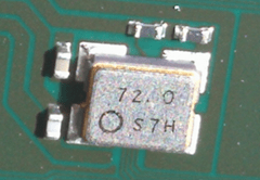
In addition, I relayed the 72MHz crystal clock cross the logic level shifter into the FPGA MRCC pin. This is for the future IMX410BQT sensor. We have this sensor in our hand but we haven’t figured out which camera it came from, presumably the new D780 DSLR. Since IMX410 in Sony A7III uses SLVS-EC, we need a reference clock for the PLL to run from. Other IOs are remapped accordingly to make room in the new layout. The reserved pads for termination resistors are removed. FPGA internal LVDS_25 DIFF_TERM works just fine for SLVS 200mV common mode.

Both sensor looks identical with the same packaging design


![3FD[[C]3)XQR]%_}7C19XLC](https://landingfield.wordpress.com/wp-content/uploads/2022/10/3fdc3xqr_7c19xlc.png?w=640&h=300 "3FD[[C]3)XQR]%_}7C19XLC")
")


