Solarpunk is all about combining that DIY hacker ethos with sustainability and renewable resources. Our usual PCB manufacturing methods, with their bevy of chemical baths and petrochemical resins aren’t exactly the most sustainable. Digging up some clay and firing it into a circuit board? Very sustainable! And apparently doable, as demonstrated by [Emily Velasco] on Mastadon.
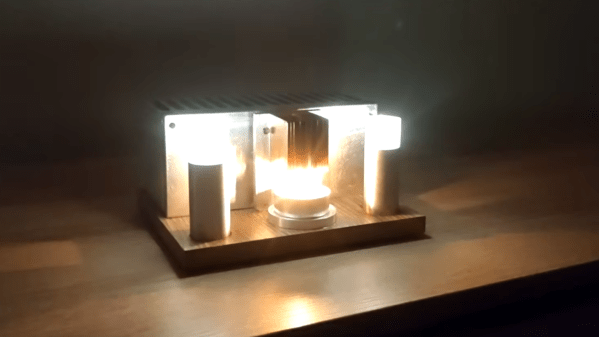
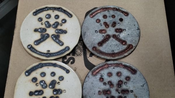
Of course anybody could take a ceramic wafer and call it a circuit board, but that’s only part of what [Emily] did. The ceramic wafer is apparently native clay, which is very cool. Even cooler is that she’s baked the traces into the pottery. While you could conceivably use some sort of conductive glaze for this, what [Emily] did was stamp her desired circuit into the unfired ceramic using a 3D-printed stamp, and then fill the depression with copper powder after the first firing. After that, a second firing is done in a reducing atmosphere to melt/sinter the copper together–it’s not totally clear which is happening here–without burning up.
The results speak for themselves; on the finished demo board, a pair of LEDs blink happily away, driven by the astable oscillator circuit baked right into the clay– and of course the components soldered to it. You’ll have to click through to see it, though.
Given those not-so-sustainable petrochemicals behind our favourite PCBs may be in short supply, this is a timely hack. If it seems familiar, that’s because we featured virtually the same technique last year, but using more-expensive silver powder instead of copper, and a campfire instead of a kiln.
Thanks to [smellsofbikes] for the tip!